By Emily Yan
The blockbuster movie Oppenheimer focuses on J. Robert Oppenheimer’s relentless pursuit behind the Manhattan Project, a critical development that resulted in the atomic bomb and helped end World War II.
Yet, a deeper look into Oppenheimer’s scientific legacy uncovers more: his significant contributions to quantum science. For instance, the Born-Oppenheimer (BO) approximation is a central concept that has influenced molecular dynamics significantly and laid the groundwork for later advancements in quantum computing by physicists such as Richard Feynman and David Deutsch.
With a projected value of US$1.3 trillion by 2035, quantum computing is becoming one of the most invested areas in tech, according to McKinsey. Behind the surge of investment is the realisation that quantum computers have the potential to dramatically accelerate research in diverse fields, such as molecular science, drug development and climate change mitigation.
In July, Google’s quantum computer performed a computation in mere seconds that would take the world’s most advanced classical supercomputer 47 years to complete. More recently, researchers have entangled 51 qubits using the Zuchongzhi quantum computer.
It seems as if each day brings news of another quantum computing breakthrough. However, beyond these headlines, what does this quantum leap mean for the electronic design automation (EDA) industry? How will it impact semiconductor device modelling? And, perhaps most importantly, how to ensure high-quality models to secure a leading position in the quantum race?
What sets quantum computing apart from classical computing
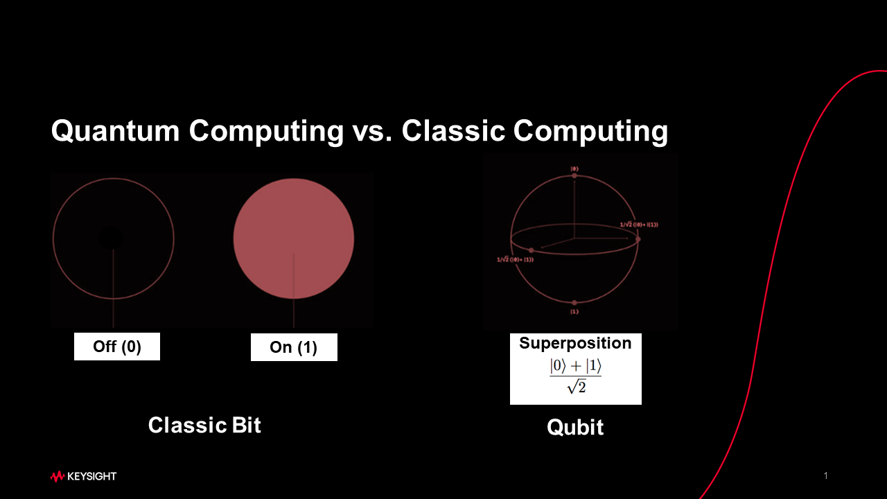
Classical computers operate using transistors, which have two states: on and off. These two states correspond to the binary data units known as bits (1 and 0). Whether you’re streaming a movie on Netflix or downloading a video game, the computer processes one set of inputs and performs one calculation at a time.
In contrast, quantum computers use quantum bits, known as qubits, to store data. Qubits exist in a state known as superposition, which allows them to represent a continuum of possible states between 1 and 0.
As shown in Figure 1, superposition can be visually depicted as the surface of a Bloch sphere. If you’re familiar with Schrödinger’s Cat, a thought experiment in which a cat is theoretically both alive and dead until observed, you’ll grasp the peculiar nature of superposition.
Superposition allows a quantum computer to perform numerous calculations with multiple inputs simultaneously. To put it simply, if we have ‘n’ qubits, a quantum computer could conduct calculations on up to 2^n different inputs at the same time. This is an exponential scaling from the one-at-a-time approach of classical computing, enabling a quantum computer to handle massive amounts of data at unprecedented speed.
How quantum computing transforms EDA
Quantum computing holds immense appeal for foundries and semiconductor companies.
First, as a quantum computer can work with multiple variables simultaneously, it has the potential to reduce complex simulations and modelling tasks from weeks to mere minutes, significantly cutting down the time-to-results (TTR).
For instance, it can solve complex optimisation problems such as layout optimisation and timing analysis more efficiently than classical computers. Last year, a team of researchers set a new record for operating a two-qubit gate in silicon in just 6.5 billionths of a second.
As the development of quantum computing accelerates, there will be an increasing demand for EDA tools capable of superconducting electronics (SCE).
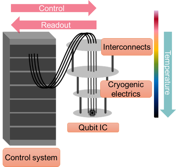
Leading companies use various types of quantum phenomena to build qubits, such as superconducting qubits, trapped ions, semiconductor spins, and photons. Designers need to integrate those qubits into a qubit IC to connect them with control and readout signals.
There are still a lot of unknowns to preparing designs that can both scale quantum computing applications and be resilient against sensitivity to fabrication variation. This advancement could catalyse the emergence of a new market segment within the EDA industry, dedicated to quantum-specific tools.
Understanding key challenges in device modelling for quantum computing
A fundamental priority for a device modelling engineer is to create accurate models of semiconductor devices, even under quantum conditions.
With the rapidly-evolving quantum race comes a set of complex challenges in the realm of device modelling.
Device modelling in cryogenic temperatures
The superposition state of a qubit is extremely delicate, which can be easily disrupted by external interference. As a result, most quantum computing systems demand high levels of isolation from electromagnetic environments and often operate under cryogenic temperatures (-130 degrees Fahrenheit or less).
Traditional semiconductor manufacturing for ICs typically operates within a temperature range of -40°F to 347°F (233.15 to 448.15 Kelvin), while quantum computing systems require cryogenic conditions, plunging below 100 millikelvins at the qubit IC level.
This stark contrast in operating temperatures between traditional ICs and quantum systems creates a significant challenge, as such extreme cold can cause variations in device electrical behaviour and introduce new temperature-dependent effects.
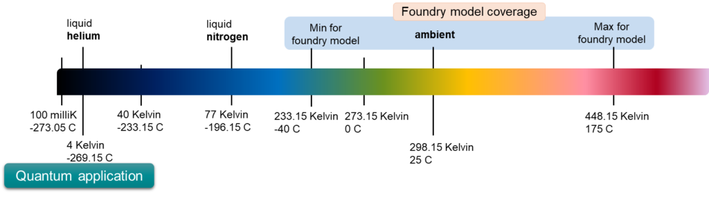
Consequently, current industry models employed in semiconductor foundries may fall short in accurately capturing device behaviour at cryogenic temperatures, leading to unanticipated design failures.
Therefore, device modelling teams are researching new ways of characterising and modelling devices to support SCE and deep cryogenic temperatures. It’s a new, cold frontier – overcoming this hurdle is essential to unlocking the full potential of quantum computing.
Developing new models for new device structures for quantum computing
Quantum applications have introduced novel device structures. Quantum phenomena, such as superposition and entanglement, introduce behaviours that aren’t accounted for in today’s industry-standard device models.
Therefore, device modelling engineers will need to code a new set of equations to accurately describe the behaviour of the new structure device, which will then be linked with commercial SPICE simulators for simulation and model parameter extraction. Extracting parameters from these new models requires not just an in-depth understanding of the models themselves but also a profound grasp of quantum devices.
Preparing for a quantum computing future
Quantum computing is a field bursting with potential, and a host of scientists and EDA companies are working tirelessly to unlock its extraordinary capabilities.
We’re on a mission to turn the immense computational power and problem-solving potential of quantum computing from concept into reality. The quantum computing future is not on the horizon – it’s unfolding right now. And the real question is: are we ready to embrace it?
Emily Yan is a product marketing manager at Keysight Technologies. Before joining Keysight, she worked on AI and big data marketing across multiple industries. Yan has an MPA degree from Columbia University and bachelor’s degrees from the University of California, Berkeley, in applied mathematics and economics.